
Manuscript accepted on :
Published online on: 09-01-2016
Plagiarism Check: Yes
S. Purushothaman*1, J. R. Dineshkumar1, S. Karthikeyan2 and S. Palpandi3
1Department of Electronics and Communication Engineering, Karpaga Vinayaga college of engineering & Technology, Maduranthagam (Tk) – 603308, Kanchipuram-Dist, TamilNadu, India. 2Department of Biomedical Engineering, Karpaga Vinayaga college of engineering & Technology, Maduranthagam (Tk)– 603308, Kanchipuram-Dist, TamilNadu, India 3Department of Computerscience and Engineering, Karpaga Vinayaga college of engineering & Technology, Maduranthagam (Tk)– 603308, Kanchipuram-Dist, TamilNadu, India
DOI : https://dx.doi.org/10.13005/bpj/828
Abstract
A novel approach converts nanoscale mechanical energy into electric energy for self-powering nanodevices that operate independently by itself without external battery for power supply requires only a power range of only μW to mW. In this work, piezoelectric p-type zinc-oxide nanowire (Sb doped ZnO NW) arrays were used to demonstrate this new approach of converting nanoscale mechanical energy like body motion, tiny mechanical vibration/disturbance etc., into electric energy.The nanogenerator (NG) using the piezoelectric effect of ZnO nanowires applies to tolerate the variable environment.In the design reported here, a piezoelectric ZnO nanowires on a flexible (Teflon) substrate and was fixed to electrodes at both surfaces. Periodically bending and releasing the substrate piezoelectric ZnO nanowires with therefore generates an alternating current,and has a number of advantages in terms of stability, robustness, cost, manufacturability and its ability to work in fluid and under harsh conditions. Here, the fundamental principle behind the nanogenerator was reviewed, and an approach for improving its performance was presented.We have implemented a simple,well controlled aqueous solution based doping strategy for synthesis of single crystalline Sb-ZnO nanowires rather using any other conventional,expensive vapour-phase synthesis methods.The Sb doping concentration was studied with ICP-OES. The morphology and structural characterizations of the Sb-ZnO NWs were performed by SEM. The crystal structure and the functional group study were done using XRD and FTIR spectroscopy. A semi conductor-confirmatory low temperature PL study of Sb doped nano wires was also carried out.
Keywords
Nanogenerator; p-type zinc-oxide nanowire arrays; piezoelectricity; self powered system
Download this article as:| Copy the following to cite this article: Purushothaman S, Dineshkumar J. R, Karthikeyan S, Palpandi S. Fabrication of Nanogenerator Using P-Type Zno Nanowires for Self Powered Wireless Data Transmission and Wearable Personal Electronics (Renewable Energy). Biomed Pharmacol J 2015;8(2) |
| Copy the following to cite this URL: Purushothaman S, Dineshkumar J. R, Karthikeyan S, Palpandi S. Fabrication of Nanogenerator Using P-Type Zno Nanowires for Self Powered Wireless Data Transmission and Wearable Personal Electronics (Renewable Energy). Biomed Pharmacol J 2015;8(2). Available from: http://biomedpharmajournal.org/?p=3834 |
Introduction
With the threatening of global warming and energy crises, searching for renewable and green energy resources is one of the most urgent challenge to sustainable development of human civilization. At the global range, TW magnitude of energy is needed, but for driving small devices, micro-watt energy is needed although the sum of the energy for running such devices in total may not be huge. The energy required for the operation of such systems is indispensible and even priceless. Different approaches have to be developed to solve the world energy problem at all scales. Photovoltaic, thermal electricity and electromagnetic induction are the well established technologies for energy harvesting, but in a case of individual sensors are difficult to get to (e.g. in hostile territory),then it may not be possible to replace batteries when required. A self sufficient power source deriving its power from the environment and thus not requiring any maintenance would be very desirable. In order for any system to be self sufficient, it must harness its energy from its surrounding environment and store this harnessed energy for later use.
There are abundant amount and types of mechanical energy exist in our living environment, such as light wind, body movement, noises, mechanical vibrations etc [1]. The Nanogenerator converts random mechanical energy into electric energy using piezoelectric nano wire arrays. The mechanism of the nano generator relies on the piezoelectric potential created in the nano wires by an external strain: a dynamic straining of the nano wire results in a transient flow of the electrons in the external load because of the driving force of the piezo potential[2, 3]. The advantage of using nano wires is that they can be triggered by tiny physical motions and the excitation frequency can be one Hz to thousands of Hz, which is ideal for harvesting random energy in the environment. Among various piezoelectric materials used for the nano generator like BaTiO3, PZT, ZnO, CdS and GaN etc.,Basically nano wires are used due to their robustness and responsiveness to tiny random mechanical disturbances. ZnO nanowires are preferred widely for these nano devices since ZnO possess the following properties includes high structural and property controllability, easy to synthesis and integrate with Si based microelectronics, high stability and extremely high elasticity, Bio-compatible, Non-toxic and Environmental friendly.
Efforts have been taken for enhancing the piezoelectricity of the nanowires which led to the development of other piezoelectric materials like p-type ZnO nanowires. Unlike the n-type semi conductive nanostructures, the mobile particle in p-type is a hole, and the electrical signal is generated from the portion of the nanostructure where the holes are accumulated. It is experimentally proved that p-type ZnO nanowires can generate the output signal near 10 times that of n-type ZnO nanowires.
Arsenic (As) and antimony (Sb) have been suggested as promising doping candidates that might produce more stable p-type conductivity and higher hole concentrations. The vertically aligned Sb-doped ZnO nanowire arrays to convert mechanical energy into electricity using materials that are environmentally friendly and biocompatible. Using the crystallographic alignment of the nanowires, a large piezo-potential is created when the nanowires are subjected to a compressive or tensile strain, which drives a transient flow of electrons in the external circuit. But this p-type doping is found to be extremely difficult so, a simple and well-controlled aqueous solution-based doping strategy for the synthesis of single-crystalline Sb-doped ZnO NWs is required.
Experimental Methods
The Nano Generator (NG) was fabricated on a flexible poly tetra fluoro ethylene (PTFE-Teflon) substrate. First, a ZnO seed layer was deposited at the selected rectangular region of 1 cm × 1 cm on the top and bottom surfaces of the substrate. The seed layer is for growing densely packed Sb doped ZnO nanowires via an aqueous solution based (wet chemical) method. A few drops of 5 mM zinc acetate ethanol solution were dropped on the PTFE substrate and blown dry. After repeating this step three times, it was baked in air for 20 min around 320 °C.
The substrate was then placed on the surface of the nutrient solution and the reaction was conducted at 90 °C for a day. The nutrient solution for growing the Sb-doped ZnO NWs was prepared by adding a certain amount of dopant solution into 25 mM sodium nitrate and 25 mM hexamethylenetetramine (HMT) before the growth. The dopant solution was prepared by mixing equal molar sodium hydroxide and glycolic acid(C2H4O3) to form sodium glycolate (NaC2H3O3), followed by dissolving antimony acetate (SbAc3) in the sodium glycolate. In all the experiments, the ratio of antimony acetate to glycolate is kept at 1:12. In a typical synthesis the amount of Sb was 0.2% in molar ratio with respect to that of zinc [4].
Then, a thin layer of poly methyl methacrylate (PMMA) was dip coated using toluene as solvent on both surfaces of the substrate at a rate of 30mm/min, followed by a 5 nm thick Au adhesion layer was deposited on the substrate by ion sputtering process on both the sides of the central rectangular area serving as the electrode of the NG.
Finally, the whole device was fully packaged with polymer support to enhance the mechanical robustness and flexibility. Two leads were connected to the top and bottom electrodes respectively using silver paste. It must be pointed out that the processing temperature is rather low (<100 ⁰C) so that the entire process is adaptable for flexible electronics [5].
Results and Discussion
XRD Analysis
The phase purity of the as-prepared samples were analyzed by X-Ray diffraction (XRD) analysis.XRD data was collected on the samples by PANanalytical X’pert diffractometer with Cu-Kα radiation (λ = 1.54 Å). The obtained XRD peak profiles were compared with standard XRD reference patterns of Sb-ZnO (JCPDS#882119) from International Center for Diffraction Data and thus the presence of Sb,ZnO and Sb-ZnO were inferred.
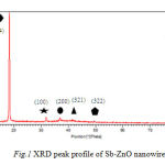 |
Figure 1: XRD peak profile of Sb-ZnO nanowires |
SEM Analysis
The nanostructure of Sb-ZnO nanowires synthesized through the step wise aqueous solution method were examined by scanning electron microscopy (SEM) and following conclusions were arrived. Initially the ZnO seed layer formed was observed using SEM,which showed a densely packed nanostructures of ZnO as illustrated in the figure 2.=
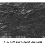 |
Figure 2: SEM image of ZnO Seed Layer |
After the growth of Sb doped ZnO NWs by the aqueous solution method,the observed SEM image revealed arrays of Sb doped ZnO NWs as illustrated below:
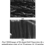 |
Figure 3: SEM image of Sb doped ZnO Nanowires @ a magnification scale of (a) 50 microns (b) 10 microns |
After dip coating PMMA on the grown Sb doped ZnO Nanowires and then ion-sputter deposition of Au on the PMMA coated Sb doped ZnO Nanowires, the surface morphologies were observed as below:
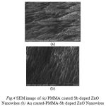 |
Figure 4: SEM image of (a) PMMA coated Sb doped ZnO Nanowires (b) Au coated-PMMA-Sb doped ZnO Nanowires |
FTIR Analysis
The evaluation of the molecular structure of Sb-ZnO nanowires and the subsequent coatings were investigated by FTIR studies. The analysis was done within the range of 400 – 2000 cm-1.
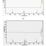 |
Figure 5: FTIR spectra of (a) Sb-ZnO nanowires (b) PMMA coated Sb doped ZnO Nanowires |
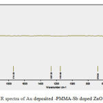 |
Figure 6: FTIR spectra of Au deposited -PMMA-Sb doped ZnO Nanowires |
Measurements were carried out in the reflection mode. The absorption peaks at 450, 436 and 456 cm-1 are due to the presence of ZnO in the Sb-ZnO, PMMA+Sb-ZnO,Au+PMMA+Sb-ZnO substrates.The presence of dopant Sb was confirmed by the absorption peaks at 674,688 and 679 cm-1 in the above mentioned stages of growth on the substrate. The peaks around 1150 cm-1 ~ 1250 cm-1 bands indicates the stretching C-O-C vibration of PMMA, 1700~ 1750cm-1 bands indicates stretching vibration of C=O groups[7].
PL Analysis
Optical studies were carried out for the grown Sb-ZnO nanowires in spectroflurometer RF-5301. The excitation wavelength was chosen as 325 nm.
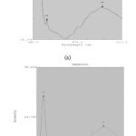 |
Figure 7: PL spectra of (a) undoped ZnO nanowires (b) Sb doped ZnO nanowires |
The PL spectra undoped ZnO nanowires exhibited strong emission intensity 100.822 at 381nm due to the band edge luminescence and a broad defect band was formed with an intensity of 123.275 at 543nm.In the case of Sb doped ZnO nanowires the PL spectra showed strong emission intensity 44.009 at 381nm due to the band edge luminescence, an emission band at 409nm was found due to the interstitial Zn in the ZnO,and a broad defect band was formed with an intensity of 57.195 at 539nm.
ICP-OES
Initially Blank solution (2%HNO3) was injected into the ICP. For analysis Sb and Zn were selected. The spectral display shows the metals and their concentration in the blank solution. Each element emitted particular wavelength.Next to blank solution, standard solution of 10 ppm (10 mg/l) was injected .The following spectral display show presence of metals and their concentration in the standard solution. Since 10 ppm was used, the metals concentrations in the solution were 10mg/l. These two analyses blank and standard were done for ICP-OES calibration purpose. Based on the results calibration curves were plotted for each element. After calibration, the synthesized samples were injected to confirm the presence of Sb and Zn resulting in spectral and calibration displays confirming the presence of desired elements.
Table 1: ICP-OES Result
| Sample ID | Analyte | Mean |
| Sample 001 | Sb 206.836 | 1.346 mg/L |
| Zn 206.200 | 9.957 mg/L |
Summary and Conclusion
In summary, a simple aqueous solution-based method for controlled doping of Sb atoms into a ZnO nanowire (NW) lattice for large scale synthesis of uniformly aligned Sb-ZnO nanowires was demonstrated. Good NW morphology with a controlled antimony doping concentration was successfully achieved. The doping concentration was studied with ICP-OES. The morphology and structural characterizations of the ZnO NWs were done by SEM. The crystal structure and the functional group study were done using XRD and FTIR spectroscopy. Also a semi conductor-confirmatory low temperature PL study of Sb doped NWs was performed. Since this method of growth of Sb-ZnO nanowire NGs has potential applications in wireless biosensing, environmental/infrastructure monitoring, sensor networks, personal electronics, a self-powered wireless data transmission system can be built as a future work.
References
- J. A. Paradiso, and T. Starner, IEEE Pervasive Comput. 4, (January 2005) 18–27.
- Z. L. Wang, and J. H. Song, Science 312, (2006) 242–246.
- X. D.Wang, J. H.Song, J. Liu & Z. L. Wang, Science 316, (2007) 102–105.
- FeiWang, Jung-Hun Seo, Dylan Bayerl, Jian Shi, Hongyi Mi, Zhenqiang Ma, Deyin Zhao, Yichen Shuai, Weidong Zhou and XudongWang, Nanotechnology 22, 225602 (2011) (8pp).
- Youfan Hu,Yan Zhang, Chen Xu, Long Lin, Robert L. Snyder, and Zhong Lin Wang, Nano Lett. 11, (2011) 2572–2557.
- Sheng Xu, Yong Qin, Chen Xu, Yaguang Wei, Rusen Yang and Zhong Lin Wang,Nature Nanotechnology,5, (May 2010) 366-373.
- R.Y. Hong, J.Z. Qian, J.X. Cao, Powder Technology 163 (2006) 160–168.

